
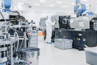
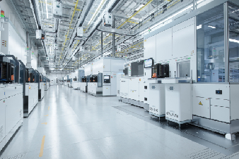
Semiconductor Capital Equipment
With decades of experience in driving state-of-the-art innovation and deploying engineering solutions worldwide, LTTS is the preferred partner for leading global semiconductor equipment manufacturers. Our range of offerings encompass the complete semiconductor capital equipment manufacturing lifecycle – from creating fabs to wafer inspections.

LTTS Offerings
Mask Manufacturing
- Mask Template Creation Optical
- Proximity Correction
- Inspection and Metrology
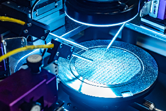
Wafer Manufacturing
- Crystal Growth
- Wafer Slicing, Grinding
- Etching, Polishing
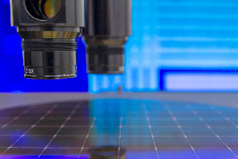
Front End
- Cleaning
- Oxidation, Deposition Lithography
- Ion Deposition
- Inspection
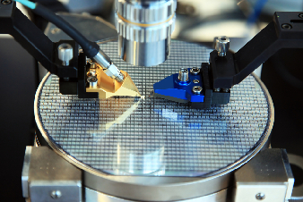
Water Testing
- Wafer Probe Test
- Multi Cell Test
Back End
- Polish Grinding / Dicing
- Wafer Mounting, Bonding, Molding
- Inspection
Cleanroom Solutions
- Storage and Material Handling Systems
- Contamination Control
- Fluid Control
Our Services

Design Services
- Mechanical Design
- Semi-Compliant Product Design
- Power Electronics and Drives Design
- Industrial and Custom Control Systems Design
- Electrical and Electromechanical Design

Digital Enablers
- Monitoring and Tracking
- Management and Maintenance
- Production Support

Ancillary Services
- Value Engineering
- Maintenance and Upgrades
- Sustenance

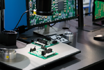
Testing and Certification Services
- Product Testing and Certification
- Test Execution and Management
The LTTS Edge
The LTTS Advantage
LTTS empowers leading global semiconductor companies to revolutionize their business paradigms through:
- Decades worth of domain expertise across innovative solutions.
- State-of-the-art lab infrastructure for advanced research and development.
- Pioneering investments across benchmark-setting motion controllers.
- Deep knowledge of SEMI standards, coupled with expertise in industrial protocols.
- A robust global pool of precision machine design SMEs, delivering exceptional engineering precision.
- Comprehensive industrial protocol expertise across seamless system integration and operations.

Success Stories
Revamp of 20-Year-Old Loadport
Our team redesigned a 20-year-old load port using modern technology and made it cost-competitive. This solution aided in the following areas: a wafer environment that is always clean ...
Know More
Wafer Processing Station
We assisted our customer, a semiconductor capital equipment manufacturing company located in the United States, to tune their indexer arm using MATLAB.
Know More
Resources
Oil and Gas
L&T Technology Services brings over 80 years of field experience in the O&G ecosystem.